Pin Headers: Difference between revisions
Jump to navigation
Jump to search
(Created page with 'There are ten sets of pin headers on the board. Enumerating them counterclockwise, starting at the top left, these are: == <span class="mw-headline"> J1D2, J2D1, J2D2 </span> ==…') |
imported>Tuxuser m (Text replace - "Category:Hardware" to "Category:Xbox360_Hardware") |
||
| (6 intermediate revisions by 4 users not shown) | |||
| Line 1: | Line 1: | ||
There are ten sets of pin headers on the board. | {{Cleanup}} | ||
There are ten sets of pin headers on the board. | |||
They are numbered according to the PCB sections (J ''X'' ''Y'' ''N''). | |||
[[File:HeaderLocations.png]] | |||
{| class="wikitable" border="0" cellspacing="2" cellpadding="2" | |||
|- | |||
! style="border-bottom:2px solid gray;" | ID | |||
! style="border-bottom:2px solid gray;" | #Pins | |||
! style="border-bottom:2px solid gray;" | Purpose | |||
|- | |||
| J1D2 | |||
| 9 | |||
| XDK Debug Header #2 | |||
|- | |||
| J1F1 | |||
| 6 | |||
| Southbridge LED Header | |||
|- | |||
| J2B1 | |||
| 13 | |||
| XDK Debug header | |||
|- | |||
| J2D1 | |||
| 6 | |||
| Southbridge Header | |||
|- | |||
| J2D2 | |||
| 8 | |||
| GPU Header | |||
|- | |||
| J5C1 | |||
| 6 | |||
| ANA Header | |||
|- | |||
| J5C2 | |||
| 6 | |||
| GPU SPI EEPROM Header | |||
|- | |||
| J7F1 | |||
| 6 | |||
| CPU SPI EEPROM Header | |||
|- | |||
| J7G1 | |||
| 3 | |||
| Aux Power Header | |||
|- | |||
| J8C1 | |||
| 10 | |||
| CPU JTAG Header | |||
|- | |||
|} | |||
== <span class="mw-headline"> J1D2, J2D1, J2D2 </span> == | == <span class="mw-headline"> J1D2, J2D1, J2D2 </span> == | ||
| Line 117: | Line 169: | ||
<br /> scheme: http://people.zeelandnet.nl/kbgeldof/j2b1_conn.JPG | <br /> scheme: http://people.zeelandnet.nl/kbgeldof/j2b1_conn.JPG | ||
[[Category:Xbox360_Hardware]] | |||
Latest revision as of 00:24, 7 January 2014
|
|
This page needs to be cleaned up, because its either hard to read or contains very little information. You can help Free60 by editing this page and cleaning it up. |
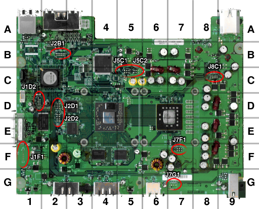
There are ten sets of pin headers on the board. They are numbered according to the PCB sections (J X Y N).
| ID | #Pins | Purpose |
|---|---|---|
| J1D2 | 9 | XDK Debug Header #2 |
| J1F1 | 6 | Southbridge LED Header |
| J2B1 | 13 | XDK Debug header |
| J2D1 | 6 | Southbridge Header |
| J2D2 | 8 | GPU Header |
| J5C1 | 6 | ANA Header |
| J5C2 | 6 | GPU SPI EEPROM Header |
| J7F1 | 6 | CPU SPI EEPROM Header |
| J7G1 | 3 | Aux Power Header |
| J8C1 | 10 | CPU JTAG Header |
J1D2, J2D1, J2D2
| J1D2 | Pin | Signal | Description |
|---|---|---|---|
| 1 | Unknown | ||
| 2 | Unknown | ||
| 3 | Unknown | ||
| 4 | Unknown | ||
| 5 | Unknown | ||
| 6 | Unknown | ||
| 7 | Unknown | ||
| 8 | GND | Ground | |
| 9 | GND | Ground |
| J2D1 | Pin | Signal | Description |
|---|---|---|---|
| 1 | Unknown | ||
| 2 | Unknown | ||
| 3 | Unknown | ||
| 4 | Unknown | ||
| 5 | Unknown | ||
| 6 | GND | Ground |
| J2D2 | Pin | Signal | Description |
|---|---|---|---|
| 1 | Unknown | ||
| 2 | Unknown | ||
| 3 | Unknown | ||
| 4 | Unknown | ||
| 5 | Unknown | ||
| 6 | GND | Ground | |
| 7 | Unknown | ||
| 8 | Unknown |
