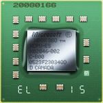
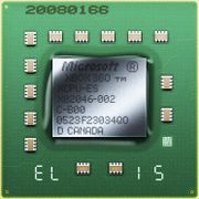
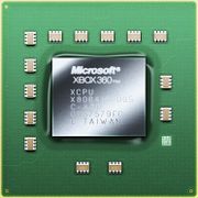
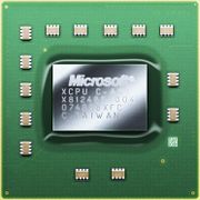
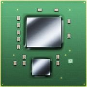
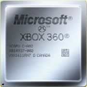
XCPU
The Microsoft XCPU is the CPU used in all Xbox 360 board revisions. It is based on IBM's PowerPC instruction set architecture. The XCPU contains 3 processor cores with each supporting two symmetric hardware threads. Each core 32KiB of L1 instruction cache and 32KiB of L1 data cache.
The XCPU was developed by Microsoft and IBM under the project codenamed "Waternoose" (from Henry J. Waternoose III in Monsters, Inc.) Its development was announced on 2003-11-03.
History
Hardware
The Xbox 360 S introduced the XCGPU, which integrated the Xenon CPU and the Xenos GPU onto the same die, and the eDRAM into the same package. The XCGPU follows the trend started with the integrated EE+GS in PlayStation 2 Slimline, combining CPU, GPU, memory controllers and IO in a single cost-reduced chip. It also contains a "front side bus replacement block" that connects the CPU and GPU internally in exactly the same manner as the front side bus would have done when the CPU and GPU were separate chips, so that the XCGPU doesn't change the hardware characteristics of the Xbox 360.
XCGPU contains 372 million transistors and is manufactured by GlobalFoundries on a 45 nm process. Compared to the original chipset in the Xbox 360 the combined power requirements are reduced by 60% and the physical chip area by 50%.[1][2]
Specifications
- 90 nm process,[3] 65 nm process upgrade in 2007[4] (codenamed "Falcon", later "Jasper"), 45 nm process since Xbox 360 S model[5]
- 165 million transistors
- Three cores, each two-way SMT-capable and clocked at 3.2 GHz[3]
- SIMD: Two VMX128 units with a dedicated (128×128 bit) register file for each core,[3] one for each thread
- 1 MB L2 cache[3] (lockable by the GPU) running at half-speed (1.6 GHz) with a 256-bit bus
- 51.2 GB/s of L2 memory bandwidth (256 bit × 1600 MHz)
- 21.6 GB/s front-side bus (On the CPU side, this interfaces to a 1.35 GHz, 8B wide, FSB dataflow; on the GPU side, it connects to a 16B wide FSB dataflow running at 675 MHz.)[3]
- Dot product performance: 9.6 billion per second
- In-order instruction execution[3]
- 768 bits of IBM eFUSE-based OTP memory[6]
- ROM (and 64 KB SRAM) storing Microsoft's Secure Bootloader, and encryption hypervisor[6]
- Big-endian architecture
References
- ↑ Jon Stokes, Ars Technica (August 24, 2010). Microsoft beats Intel, AMD to market with CPU/GPU combo chip. Retrieved on August 24, 2010.
- ↑ PC Perspective (June 21, 2010). The New Xbox 360 S "Slim" Teardown: Opened and Tested. Archived from the original on June 25, 2010. Retrieved on June 24, 2010.
- ↑ 3.0 3.1 3.2 3.3 3.4 3.5 Jeffrey Brown (December 6, 2005). Application-customized CPU design: The Microsoft Xbox 360 CPU story. Archived from the original on October 25, 2007. Retrieved on September 8, 2007.
- ↑ César A. Berardini (August 21, 2006). Chartered to Manufacture 65-nm Xbox 360 CPUs. Archived from the original on January 23, 2008. Retrieved on January 9, 2008.
- ↑ Patel, Nilay (June 14, 2010). New Xbox 360 looks angular and Ominous. Engadget.com. Retrieved on June 14, 2010.
- ↑ 6.0 6.1 Xbox360 security system.
Gallery
| ||||||||||||||||||||||||||||||||||||||||||||||||||
